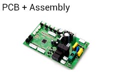
Sunthone offers one-stop PCB and PCBA services, including PCB manufacturing, PCB assembly, components sourcing, stencils, cable assembly, final product assembly and testing.
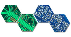
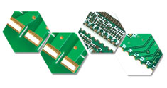
Multilayer PCBs greatly increase the area available for the wiring with one or more conductor pattern inside the board. This is achieved by gluing (laminating) several double-sided boards together with insulating layers in between. The number of layers is referred to as the number of separate conductor patterns.

Type of Assembly: SMT, THT, hand soldering, mixed assembly. SMT Sides: single side SMT, double side SMT. Min Assembly Package: 0201 passive components
Components Packaging: tape, cut tape, tube, reel, loose parts
Testing: AOI, X-RAY, In-circuit Test, functional test, aging test
Mounting Precision: 0.1mm
Mounting Capacity: 2million points

Type of Assembly: SMT, THT, hand soldering, mixed assembly. Solder Type: RoHS and lead free solder, leaded solder, conformal coating. SMT Sides: single side SMT, double side SMT
Components Packaging: tape, cut tape, tube, reel, loose parts
Testing: AOI, X-RAY, In-circuit Test, functional test, aging test
Mounting Precision: 0.1mm
Mounting Capacity: 2million points

Type of Assembly: SMT, THT, hand soldering, mixed assembly
Solder Type: RoHS and lead free solder, leaded solder, conformal coating
SMT Sides: single side SMT, double side SMT
Min Assembly Package: 0201 passive components
Components Packaging: tape, cut tape, tube, reel, loose parts
Mounting Precision: 0.1mm
Mounting Capacity: 2million points

Type of Assembly: SMT, THT, hand soldering, mixed assembly. Solder Type: RoHS and lead free solder, leaded solder, conformal coating. SMT Sides: single side SMT, double side SMT
Min Assembly Package: 0201 passive components
Components Packaging: tape, cut tape, tube, reel, loose parts
Testing: AOI, X-RAY, In-circuit Test, functional test, aging test
Mounting Capacity: 2million points

Type of Assembly: SMT, THT, hand soldering, mixed assembly
Solder Type: RoHS and lead free solder, leaded solder, conformal coating
SMT Sides: single side SMT, double side SMT
Components Packaging: tape, cut tape, tube, reel, loose parts
Testing: AOI, X-RAY, In-circuit Test, functional test, aging test
Mounting Precision: 0.1mm
Mounting Capacity: 2million points

Type of Assembly: SMT, THT, hand soldering, mixed assembly
Solder Type: RoHS and lead free solder, leaded solder, conformal coating
SMT Sides: single side SMT, double side SMT
Min Assembly Package: 0201 passive components
Testing: AOI, X-RAY, In-circuit Test, functional test, aging test
Mounting Precision: 0.1mm
Mounting Capacity: 2million points

Material: FR-4
Layer: 4
Board thickness: 1.6mm
Copper weight: 1Oz
Min trace/clearance: 0.25/0.25mm
Min hole size: 0.3mm
Surface finish: Lead free HASL
Specialty:
Application: Industrial Facilities

Material: FR-4
Layer: 4
Board thickness: 1.6mm
Copper weight: 1Oz
Min trace/clearance: 0.25/0.2mm
Min hole size: 0.25mm
Surface finish: Immersion Gold
Specialty:
Application: Power Supply

Material: FR-4
Layer: 4
Board thickness: 1.5mm
Copper weight: 1Oz
Min trace/clearance: 0.15/0.15mm
Min hole size: 0.2mm
Surface finish: Immersion Gold
Specialty:
Application: Telecommunications

Material: FR-4
Layer: 6
Board thickness: 1.6mm
Copper weight: 1Oz
Min trace/clearance: 0.15/0.15mm
Min hole size: 0.25mm
Surface finish: Immersion Gold
Specialty:
Application: Industrial Facilities

Material: FR-4
Layer: 6
Board thickness: 1.6mm
Copper weight: 1Oz
Min trace/clearance: 0.075/0.075mm
Min hole size: 0.2mm
Surface finish: Lead free HASL
Specialty: fine trace/clearance
Application: Industrial Facilities

tiesMaterial: FR-4
Layer: 10
Board thickness: 1.6mm
Copper weight: 1Oz
Min trace/clearance: 0.075/0.075mm
Min hole size: 0.25mm
Surface finish: Lead free HASL
Specialty: Impedance Control + fine trace/clearance
Application: Industrial Facilities
We work with our customer towarding success with superior quality PCBs provided at a low cost. We fully understand your need for high quality PCBs delivered on time to build your products. In addition, we want to lower your costs so your business endeavors are more profitable.

Material: FR-4
Layer: 2
Board thickness: 1.0mm
Copper weight: 1Oz
Min trace/clearance: 0.25/0.25mm
Min hole size: 0.2mm
Surface finish: Immersion Gold
Specialty: Plated Half-holes
Application: Communications

Material: FR-4
Layer: 2
Board thickness: 1.2mm
Copper weight: 1Oz
Min trace/clearance: 0.2/0.2mm
Min hole size: 0.25mm
Surface finish: Lead free HASL
Specialty:
Application: GPS Terminals

Material: FR-4
Layer: 1
Board thickness: 1.6mm
Copper weight: 1Oz
Min trace/clearance: 0.51/0.38mm
Min hole size: 0.762mm
Surface finish: Lead free HASL
Specialty:
Application: LED

Material: FR-4
Layer: 2
Board thickness: 2.0mm
Copper weight: 2Oz
Min trace/clearance: 0.51/0.38mm
Min hole size: 0.38mm
Surface finish: Immersion Gold
Specialty: Application: Toys

Material: FR-4
Layer: 2
Board thickness: 1.6mm
Copper weight: 1Oz
Min trace/clearance: 0.15/0.15mm
Min hole size: 0.25mm Surface
finish: Immersion Gold
Specialty: Plated Edges
Application: Toys

Material: FR-4
Layer: 2 Board
thickness: 2.0mm Copper
weight: 1Oz Min trace/clearance: 0.15/0.15mm
Min hole size: 0.3mm
Surface finish: Immersion Gold
Specialty:
Application: SPA Equipments
High frequency circuit boards are developing with the increasing complexity of electronic components and switches continually requires faster signal flow rates, and thus higher transmission frequencies.

Material: Rogers
Layer: 2
Board thickness: 0.8mm
Copper weight: 1Oz
Min trace/clearance: 0.15/0.15mm
Min hole size: 0.25mm
Surface finish: immersion Gold
Specialty: Rogers material + high frequency

Material: Rogers + FR-4
Layer: 6
Board thickness: 1.6mm
Copper weight: 1Oz
Min trace/clearance: 0.1/0.1mm
Min hole size: 0.2mm
Surface finish: immersion Gold
Specialty: Rogers material + high frequency
Application: Telecommunications

Material: Rogers + FR-4
Layer: 8
Board thickness: 2.4mm
Copper weight: 1Oz
Min trace/clearance: 0.1/0.1mm
Min hole size: 0.25mm
Surface finish: Lead free HASL
Specialty: Rogers material + high frequency
Application: Telecommunications

Material: Rogers
Layer: 2
Board thickness: 0.5mm
Copper weight: 1Oz
Min trace/clearance: 0.38/0.38mm
Min hole size: 0.51mm
Surface finish: OSP
Specialty: Rogers material + high frequency
Application: Telecommunications

Material: Rogers
Layer: 2
Board thickness: 0.5mm
Copper weight: 1Oz
Min trace/clearance: 0.51/0.38mm
Min hole size: 0.51mm
Surface finish: OSP
Specialty: Rogers material + high frequency
Application: Telecommunications

Material: Rogers
Layer: 2
Board thickness: 0.5mm
Copper weight: 1Oz
Min trace/clearance: 0.51/0.38mm
Min hole size: 0.38mm
Surface finish: OSP
Specialty: Rogers material + high frequency
Application: Telecommunications
Impedance is the sum of the resistance and reactance of an electrical circuit expressed in Ohms. The resistance being the opposition to current flow present in all materials.

Material: FR-4
Layer: 2
Board thickness: 1.2mm
Copper weight: 1Oz
Min trace/clearance: 0.25/0.2mm
Min hole size: 0.3mm
Surface finish: Lead free HASL
Specialty: Impedance controlled
Application: Industrial Facilities

Material: FR-4
Layer: 4
Board thickness: 1.6mm
Copper weight: 1Oz
Min trace/clearance: 0.2/0.2mm
Min hole size: 0.25mm
Surface finish: Immersion Gold
Specialty: Impedance controlled
Application: Industrial Facilities

Material: FR-4
Layer: 8
Board thickness: 1.6mm
Copper weight: 1Oz
Min trace/clearance: 0.15/0.15mm
Min hole size: 0.25mm
Surface finish: Immersion Gold
Specialty: Impedance controlled + BGA
Application: Industrial Facilities

Material: FR-4
Layer: 2
Board thickness: 1.6mm
Copper weight: 1Oz
Min trace/clearance: 0.2/0.2mm
Min hole size: 0.25mm
Surface finish: Immersion Gold
Specialty: Impedance controlled + BGA
Application:

Material: FR-4
Layer: 6
Board thickness: 1.0mm
Copper weight: 1Oz
Min trace/clearance: 0.1/0.1mm
Min hole size: 0.2mm
Surface finish: Immersion Gold
Specialty: Impedance controlled + BGA
Application: Telecommunications
Material: FR-4
Layer: 2
Board thickness: 1.6mm
Copper weight: 1Oz
Min trace/clearance: 0.2/0.2mm
Min hole size: 0.25mm
Surface finish: OSP
Specialty: Impedance controlled + BGA
Application:
Heavy copper does not have a set definition per IPC. However, the industry generally accepts the definition to be the use of 3 ounce copper or higher in inner and/or outer layers of a printed circuit or power distribution board.

Material: FR-4
Layer: 4
Board thickness: 1.6mm
Copper weight: 2Oz
Min trace/clearance: 0.25/0.2mm
Min hole size: 0.5mm
Surface finish: Immersion Gold
Specialty: Heavy Copper Application: Power Supply

Material: FR-4
Layer: 4
Board thickness: 1.6mm
Copper weight: 2Oz
Min trace/clearance: 0.25/0.25mm
Min hole size: 0.38mm
Surface finish: Lead free HASL
Specialty: Heavy Copper
Application: Power Supply

Material: FR-4
Layer: 2
Board thickness: 1.6mm
Copper weight: 4Oz
Min trace/clearance: 0.30/0.25mm
Min hole size: 0.4mm Surface finish: Lead free HASL
Specialty: Heavy Copper
Application: Power Supply

Material: FR-4
Layer: 2
Board thickness: 2.0mm
Copper weight: 4Oz
Min trace/clearance: 0.30/0.25mm
Min hole size: 0.5mm
Surface finish: Lead free HASL
Specialty: Heavy Copper
Application: Power Supply

Material: FR-4
Layer: 2
Board thickness: 2.0mm
Copper weight: 3Oz
Min trace/clearance: 0.25/0.3mm
Min hole size: 0.3mm
Surface finish: Immersion Gold
Specialty: Heavy Copper
Application: Power Supply

Material: FR-4
Layer: 2
Board thickness: 2.0mm
Copper weight: 3Oz
Min trace/clearance: 0.38/0.38mm
Min hole size: 0.3mm
Surface finish: Immersion Gold
Specialty: Heavy Copper
Application: Power Supply
Hard Gold is used where either a very resilient surface finish is required, or in the case of edge connectors a wear resistant oxide free finish is required.

Material: FR-4
Layer: 2
Board thickness: 1.2mm
Copper weight: 1Oz
Min trace/clearance: 0.15/0.15mm
Min hole size: 0.3mm
Surface finish: Plating Gold
Specialty: Hard Gold Plating
Application: Household Articles

Material: FR-4
Layer: 4
Board thickness: 1.2mm
Copper weight: 1Oz
Min trace/clearance: 0.51/0.38mm
Min hole size: 0.38mm
Surface finish: Plating Gold
Specialty: Hard Gold Plating
Application: Household Articles

Material: FR-4
Layer: 4
Board thickness: 1.0mm
Copper weight: 1Oz
Min trace/clearance: 0.15/0.15mm
Min hole size: 0.25mm
Surface finish: Plating Gold
Specialty: Hard Gold Plating
Application: Consumer electronics

Material: FR-4
Layer: 2
Board thickness: 1.5mm
Copper weight: 1Oz
Min trace/clearance: 0.1/0.1mm
Min hole size: 0.2mm
Surface finish: Plating Gold
Specialty: Hard Gold Plating
Application: Consumer electronics

Material: FR-4
Layer: 2
Board thickness: 1.0mm
Copper weight: 1Oz
Min trace/clearance: 0.25/0.25mm
Min hole size: 0.2mm
Surface finish: Plating Gold
Specialty: Hard Gold Plating
Application: Consumer electronics

Material: FR-4
Layer: 2
Board thickness: 1.6mm
Copper weight: 1Oz
Min trace/clearance: 0.31/0.25mm
Min hole size: 0.5mm
Surface finish: Plating Gold + Carbon Ink
Specialty: Hard Gold Plating
Application: Remote Control
Gold Finger PCB refers to those PCBs with finger-like pads applying plated gold surface finish, and they are usually used as edge-connectors.

Material: FR-4
Layer: 4
Board thickness: 2.0mm
Copper weight: 1Oz
Min trace/clearance: 0.2/0.2mm
Min hole size: 0.25mm
Surface finish: Immersion Gold + Gold Finger
Specialty: Gold Finger
Application:

Material: FR-4
Layer: 4
Board thickness: 1.6mm
Copper weight: 1Oz
Min trace/clearance: 0.15/0.15mm
Min hole size: 0.2mm
Surface finish: Lead free HASL + Gold Finger
Specialty: Fine Gold Fingers and Fine clearance between fingers

Material: FR-4
Layer: 6
Board thickness: 1.6mm
Copper weight: 1Oz
Min trace/clearance: 0.15/0.15mm
Min hole size: 0.2mm
Surface finish: Lead free HASL + Gold Finger
Specialty: Fine Gold Fingers and Fine clearance between fingers

Material: FR-4
Layer: 2
Board thickness: 1.6mm
Copper weight: 1Oz
Min trace/clearance: 0.38/0.25mm
Min hole size: 0.3mm
Surface finish: Immersion Gold + Gold Finger
Specialty: Gold Fingers
Application:

Material: FR-4
Layer: 2
Board thickness: 1.6mm
Copper weight: 1Oz
Min trace/clearance: 0.38/0.38mm
Min hole size: 0.51mm
Surface finish: Lead free HASL + Gold Finger
Specialty: Gold Fingers
Application: counter card
Blind Vias start on an outer layer but terminate on an inner layer. Buried Vias exist only between inner layers and do not begin or terminate on an outer layer.

Material: FR-4
Layer: 6
Board thickness: 1.6mm
Copper weight: 1Oz
Min trace/clearance: 0.1/0.1mm
Min hole size: 0.2mm Surface finish: Immersion Gold
Specialty: Blind and Buried Vias + BGA + Impedance Control
Application: Telecommunications

Material: FR-4
Layer: 8
Board thickness: 1.6mm
Copper weight: 1Oz
Min trace/clearance: 0.1/0.1mm
Min hole size: 0.2mm
Surface finish: Immersion Gold + Gold Fingers
Specialty: Blind and Buried Vias + BGA + Impedance Control + Gold Fingers
Application: Industrial Computer

Material: FR-4
Layer: 8
Board thickness: 1.6mm
Copper weight: 1Oz
Min trace/clearance: 0.1/0.1mm
Min hole size: 0.2mm
Surface finish: Immersion Gold
Specialty: Blind and Buried Vias + BGA + Impedance Control
Application: Industrial Computer

Material: FR-4
Layer: 6
Board thickness: 1.6mm
Copper weight: 1Oz
Min trace/clearance: 0.15/0.15mm
Min hole size: 0.2mm
Surface finish: Lead free HASL
Specialty: Blind and Buried Vias + BGA
Application: Industrial Facilities

Material: FR-4 Tg=170
Layer: 6
Board thickness: 1.6mm
Copper weight: 1Oz
Min trace/clearance: 0.15/0.15mm
Min hole size: 0.25mm
Surface finish: Immersion Gold + Carbon Ink
Specialty: Blind and Buried Vias
Application: Medical Facilities

Material: FR-4
Layer: 4
Board thickness: 1.6mm
Copper weight: 1Oz
Min trace/clearance: 0.51/0.38mm
Min hole size: 0.51mm
Surface finish: Immersion Gold
Specialty: blind and buried vias
Application:
Plated half-holes are predominantly used for board-on-board connections, mostly where two printed circuit boards with different technologies are combined. E.g. the combination of complex microcontroler modules with common, individually designed PCBs.

Material: FR-4
Layer: 2
Board thickness: 1.6mm
Copper weight: 1Oz
Min trace/clearance: 1.5/1.5mm
Min hole size: 0.76mm
Surface finish: Immersion Gold
Specialty: Plated Half-holes
Application: Power Supply

Material: FR-4
Layer: 4
Board thickness: 1.6mm
Copper weight: 1Oz
Min trace/clearance: 0.2/0.2mm
Min hole size: 0.25mm
Surface finish: Immersion Gold
Specialty: Plated Half-holes
Application: Communications

Material: FR-4
Layer: 4
Board thickness: 1.6mm
Copper weight: 1Oz
Min trace/clearance: 0.15/0.15mm
Min hole size: 0.2mm
Surface finish: Immersion Gold
Specialty: Plated Half-holes
Application: Communications

Material: FR-4
Layer: 2
Board thickness: 1.6mm
Copper weight: 1Oz
Min trace/clearance: 0.25/0.25mm
Min hole size: 0.3mm
Surface finish: Immersion Gold
Specialty: Plated Half-holes
Application: Communications

Material: FR-4
Layer: 2
Board thickness: 1.6mm
Copper weight: 1Oz
Min trace/clearance: 0.25/0.25mm
Min hole size: 0.3mm
Surface finish: Immersion Gold
Specialty: Plated Half-holes
Application: Household Articles
Material: FR-4
Layer: 4
Board thickness: 1.6mm
Copper weight: 1Oz
Min trace/clearance: 0.25/0.25mm
Min hole size: 0.3mm
Surface finish: Immersion Gold
Specialty: Plated Half-holes
Application: Communications
PCB Manufacturer, PCB Supplier, PCB & PCBA,Bonding PCB board manufacturer in china.With excellent performance on quality and lead time, Sunthone can be your best partner, either you are a factory or trader from east or west.

Material: FR-4
Layer: 2
Board thickness: 1.6mm
Copper weight: 1Oz
Min trace/clearance: 0.2/0.2mm
Min hole size: 0.3mm
Surface finish: Immersion Gold
Specialty: Bonding Pads
Application: LCD module products

Material: FR-4
Layer: 2
Board thickness: 1.6mm
Copper weight: 1Oz
Min trace/clearance: 0.15/0.15mm
Min hole size: 0.3mm
Surface finish: Immersion Gold
Specialty: Bonding Pads
Application: LCD module products

Material: FR-4
Layer: 2
Board thickness: 1.6mm
Copper weight: 1Oz
Min trace/clearance: 0.2/0.2mm
Min hole size: 0.3mm
Surface finish: Immersion Gold
Specialty: Bonding Pads
Application: LCD module products

Material: FR-4
Layer: 2
Board thickness: 1.6mm
Copper weight: 1Oz
Min trace/clearance: 0.2/0.15mm
Min hole size: 0.3mm
Surface finish: Immersion Gold
Specialty: Bonding Pads
Application: LCD module products

Material: FR-4
Layer: 2
Board thickness: 1.6mm
Copper weight: 1Oz
Min trace/clearance: 0.2/0.2mm
Min hole size: 0.3mm
Surface finish: Immersion Gold
Specialty: Bonding Pads
Application: LCD module products

Material: FR-4
Layer: 2
Board thickness: 1.6mm
Copper weight: 1Oz
Min trace/clearance: 0.15/0.15mm
Min hole size: 0.3mm
Surface finish: Immersion Gold
Specialty: Bonding Pads
Application: LCD module products
PCB Manufacturer, PCB Supplier, PCB & PCBA,Unconventional Thickness PCB board manufacturer in china.The company focuses on major markets including Domestic Market, America, Europe, Oceania, Southeast Asia and Middle East.

Material: FR-4
Layer: 10
Board thickness: 3.0mm
Copper weight: 1Oz
Min trace/clearance: 0.1/0.1mm
Min hole size: 0.3mm
Surface finish: Lead free HASL
Specialty:
Application: Industrial Facilities

Material: FR-4
Layer: 2
Board thickness: 3.0mm
Copper weight: 1Oz
Min trace/clearance: 0.15/0.15mm
Min hole size: 0.3mm
Surface finish: Lead free HASL
Specialty:
Application: Industrial Facilities

Material: FR-4
Layer: 2
Board thickness: 3.0mm
Copper weight: 1Oz
Min trace/clearance: 0.15/0.15mm
Min hole size: 0.3mm
Surface finish: Lead free HASL
Specialty:
Application: Industrial Facilities

Material: FR-4
Layer: 2
Board thickness: 0.4mm
Copper weight: 1Oz
Min trace/clearance: 0.1/0.1mm
Min hole size: 0.2mm Surface finish: Immersion Gold
Specialty: Small Board Thickness
Application: Consumer Electronics

Material: FR-4
Layer: 2
Board thickness: 0.5mm
Copper weight: 1Oz
Min trace/clearance: 0.2/0.15mm
Min hole size: 0.25mm
Surface finish: Immersion Gold
Specialty: Small Board Thickness
Application: Consumer Electronics

Material: FR-4
Layer: 4
Board thickness: 0.6mm
Copper weight: 1Oz
Min trace/clearance: 0.15/0.15mm
Min hole size: 0.25mm
Surface finish: Immersion Gold
Specialty: Small Board Thickness
Application: Consumer Electronics
Aluminium-based circuit boards are an excellent alternative to standard circuit boards, if the circuit boards are exposed to large mechanical loads, or a high level of dimensional stability is required, or high temperatures must be conducted away from power components or LED's.

Material: Aluminium
Layer: 1
Board thickness: 1.6mm
Copper weight: 1Oz
Min trace/clearance: 1.5/2.0mm
Min hole size: 2.0mm
Surface finish: Lead free HASL
Specialty: Aluminium Core
Application: LED Lightning

Material: Aluminium
Layer: 1
Board thickness: 3.0mm
Copper weight: 1Oz
Min trace/clearance: 3.0/2.5mm
Min hole size: 3.81mm
Surface finish: Lead free HASL
Specialty: Aluminium Core + Counter-sink Holes
Application: LED Lightning
Material: Aluminium
Layer: 1
Board thickness: 3.0mm
Copper weight: 1Oz
Min trace/clearance: 2.5/1.0mm
Min hole size: 2.54mm
Surface finish: Immersion Gold
Specialty: Aluminium Core + Counter-sink Holes
Application: LED Lightning

Material: Aluminium
Layer: 1
Board thickness: 1.5mm
Copper weight: 1Oz
Min trace/clearance: 1.5/1.0mm
Min hole size: 2.54mm
Surface finish: Lead free HASL
Specialty: Aluminium Core
Application: LED Lightning

Material: Aluminium
Layer: 1
Board thickness: 1.5mm
Copper weight: 1Oz
Min trace/clearance: 1.5/1.5mm
Min hole size: 3.81mm
Surface finish: Lead free HASL
Specialty: Aluminium Core
Application: LED Lightning

Material: Aluminium
Layer: 1
Board thickness: 1.5mm
Copper weight: 1Oz
Min trace/clearance: 1.0/1.0mm
Min hole size: 3.81mm
Surface finish: Lead free HASL
Specialty: Aluminium Core
Application: LED Lightning
| Technical Capacity | |||
|---|---|---|---|
| Layers | 1-24 layers | Min Board Thickness(2-layer) | 0.2mm |
| Max Panel Size | 635×1100mm | Min Board Thickness(4-layer) | 0.4mm |
| Max Copper | 12Oz | Min Inner-layer Thickness | 0.1mm |
| Min Trace | 0.075mm | Min Pad Ring | 0.1mm |
| Min Clearance | 0.075mm | Min Hole Location Tolerance | ±0.075mm |
| Min Hole Size | 0.15mm | Min Hole Size Tolerance | ±0.05mm |
| Board Twist | ≤ 1° | Min Outer Dimension Tolerance | ±0.1mm |
| Surface Finish | HAL, HASL, Immersion Gold, Plating Gold, Plating Nickel, Plating Silver, Gold Finger, OSP | ||
| Board Material | FR-4, High Tg FR-4, Halogen Free FR-4, Thick Copper FR-4, Aluminium Based | ||
|
Standard Lead Time |
2-layer samples in 3 days only 4-layer samples in 5 days only |
||
Critical for the impedances in high frequency circuit boards are principally the conductor trace geometry, the layer buildup, and the dielectric constant (er) of the materials used.
| Technical Capacity | |||
|---|---|---|---|
| Layers | 1-24 layers | Min Board Thickness(2-layer) | 0.2mm |
| Max Panel Size | 635×1100mm | Min Board Thickness(4-layer) | 0.4mm |
| Max Copper | 12Oz | Min Inner-layer Thickness | 0.1mm |
| Min Trace | 0.075mm | Min Pad Ring | 0.1mm |
| Min Clearance | 0.075mm | Min Hole Location Tolerance | ±0.075mm |
| Min Hole Size | 0.15mm | Min Hole Size Tolerance | ±0.05mm |
| Board Twist | ≤ 1° | Min Outer Dimension Tolerance | ±0.1mm |
| Surface Finish | HAL, HASL, Immersion Gold, Plating Gold, Plating Nickel, Plating Silver, Gold Finger, OSP | ||
| Board Material | FR-4, High Tg FR-4, Halogen Free FR-4, Thick Copper FR-4, Aluminium Based | ||
|
Standard Lead Time |
2-layer samples in 3 days only 4-layer samples in 5 days only |
||
The typical design considerations involved in the determination for controlling the impedance are the strength of the signals involved, the susceptibility of the circuit to noise and signal distortion, the criticality of signal timing and the speed at which the signal’s source is attempting to force a change in voltage and/or current.
| Technical Capacity | |||
|---|---|---|---|
| Layers | 1-24 layers | Min Board Thickness(2-layer) | 0.2mm |
| Max Panel Size | 635×1100mm | Min Board Thickness(4-layer) | 0.4mm |
| Max Copper | 12Oz | Min Inner-layer Thickness | 0.1mm |
| Min Trace | 0.075mm | Min Pad Ring | 0.1mm |
| Min Clearance | 0.075mm | Min Hole Location Tolerance | ±0.075mm |
| Min Hole Size | 0.15mm | Min Hole Size Tolerance | ±0.05mm |
| Board Twist | ≤ 1° | Min Outer Dimension Tolerance | ±0.1mm |
| Surface Finish | HAL, HASL, Immersion Gold, Plating Gold, Plating Nickel, Plating Silver, Gold Finger, OSP | ||
| Board Material | FR-4, High Tg FR-4, Halogen Free FR-4, Thick Copper FR-4, Aluminium Based | ||
|
Standard Lead Time |
2-layer samples in 3 days only 4-layer samples in 5 days only |
||
Gold Finger PCBs normally have to bevel the edge connectors to ensure easy insertion. Bevelling can be specified in the order details if there are any special instructions.
| Technical Capacity | |||
|---|---|---|---|
| Layers | 1-24 layers | Min Board Thickness(2-layer) | 0.2mm |
| Max Panel Size | 635×1100mm | Min Board Thickness(4-layer) | 0.4mm |
| Max Copper | 12Oz | Min Inner-layer Thickness | 0.1mm |
| Min Trace | 0.075mm | Min Pad Ring | 0.1mm |
| Min Clearance | 0.075mm | Min Hole Location Tolerance | ±0.075mm |
| Min Hole Size | 0.15mm | Min Hole Size Tolerance | ±0.05mm |
| Board Twist | ≤ 1° | Min Outer Dimension Tolerance | ±0.1mm |
| Surface Finish | HAL, HASL, Immersion Gold, Plating Gold, Plating Nickel, Plating Silver, Gold Finger, OSP | ||
| Board Material | FR-4, High Tg FR-4, Halogen Free FR-4, Thick Copper FR-4, Aluminium Based | ||
|
Standard Lead Time |
2-layer samples in 3 days only 4-layer samples in 5 days only |
||
The board-on-board PCBs therefore need plated half-holes, which serve as SMD connection pads. Through directly connecting the PCBs together, the whole system is considerably thinner than a comparable connection with multi-pin connectors.
| Technical Capacity | |||
|---|---|---|---|
| Layers | 1-24 layers | Min Board Thickness(2-layer) | 0.2mm |
| Max Panel Size | 635×1100mm | Min Board Thickness(4-layer) | 0.4mm |
| Max Copper | 12Oz | Min Inner-layer Thickness | 0.1mm |
| Min Trace | 0.075mm | Min Pad Ring | 0.1mm |
| Min Clearance | 0.075mm | Min Hole Location Tolerance | ±0.075mm |
| Min Hole Size | 0.15mm | Min Hole Size Tolerance | ±0.05mm |
| Board Twist | ≤ 1° | Min Outer Dimension Tolerance | ±0.1mm |
| Surface Finish | HAL, HASL, Immersion Gold, Plating Gold, Plating Nickel, Plating Silver, Gold Finger, OSP | ||
| Board Material | FR-4, High Tg FR-4, Halogen Free FR-4, Thick Copper FR-4, Aluminium Based | ||
|
Standard Lead Time |
2-layer samples in 3 days only 4-layer samples in 5 days only |
||
Additional application areas for this technology include: high current application, power LED's, SMD and power circuit boards. The high thermal conductivity permits a quick and effective transfer of the heat produced.
| Technical Capacity | |||
|---|---|---|---|
| Layers | 1-24 layers | Min Board Thickness(2-layer) | 0.2mm |
| Max Panel Size | 635×1100mm | Min Board Thickness(4-layer) | 0.4mm |
| Max Copper | 12Oz | Min Inner-layer Thickness | 0.1mm |
| Min Trace | 0.075mm | Min Pad Ring | 0.1mm |
| Min Clearance | 0.075mm | Min Hole Location Tolerance | ±0.075mm |
| Min Hole Size | 0.15mm | Min Hole Size Tolerance | ±0.05mm |
| Board Twist | ≤ 1° | Min Outer Dimension Tolerance | ±0.1mm |
| Surface Finish | HAL, HASL, Immersion Gold, Plating Gold, Plating Nickel, Plating Silver, Gold Finger, OSP | ||
| Board Material | FR-4, High Tg FR-4, Halogen Free FR-4, Thick Copper FR-4, Aluminium Based | ||
|
Standard Lead Time |
2-layer samples in 3 days only 4-layer samples in 5 days only |
||
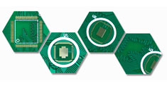
Multilayer PCB
Single-double Sided PCB
High Frequency PCB
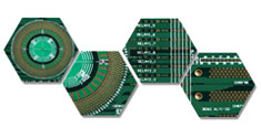
Impedance PCB
Heavy Copper PCB
Hard Gold PCB
Gold Finger PCB
Blind-buried Vias PCB
Plated Half-holes PCB
Bonding PCB
Unconventional Thickness PCB
Aluminium-based PCB