| ITEM | Capability |
| Month Capability | 1000types/month,8,000sqm/month |
| Board Material | Standard FR4: Shengyi, ITEQ, KB, GDM High TG: S1000-2, IT180 |
| Surface treatment | OSP, HASL, LF-HASL, ENIG(Chem. Gold), Immersion Tin, Immersion silver, Plating hard gold, Gold fingers,Flash gold, ENEPIG |
| Tolerance | Board thickness tolerance 1.0mm: +/-0.1mm 1.0mm-2.0mm: +/-10% >2.0mm: +/-8% |
| Hole diameter tolerance PTH: +/-0.075mm NPTH:+/-0.05mm | |
| Hole location tolerance: +/-0.075mm | |
| Outline tolerance: < 100mm: +/-0.1mm 100mm-300mm: +/-0.15mm >300mm: +/-0.2mm | |
| Technical Specification | Layers: 1-24 layers |
| Min line width/space: 0.075/0.075mm | |
| Min hole: 0.15mm (mechanical drilling) 0.1mm (laser drilling) | |
| Min pad ring: 0.1mm | |
| Max copper thickness: 12oz | |
| Max board size:1-2 layers: 635 X 1100mm Multilayers: 500 X 1100mm | |
| Board thickness: 2-layers: 0.2-7.0mm Multi-layers: 0.4-7.0mm Inner layers: 0.1mm | |
| Board warpage: ≤1° | |
| Min solder mask bridge: 0.08mm | |
| Aspect Ration: 8:1 | |
| Plugging Vias capability: 0.2-0.8mm | |
| Au, Ni thickness control: 1. Chem gold: Au:1-10u” 2. Gold fingers: Au:1-150u” 3. Flash gold: Au:1-10u” 4. Hard gold:Au:1-150u” 5. Ni thickness:50-1000u” 6. ENEPIG: Au:1-8u”,Pd:2-5u |

Auto Cutting Machine

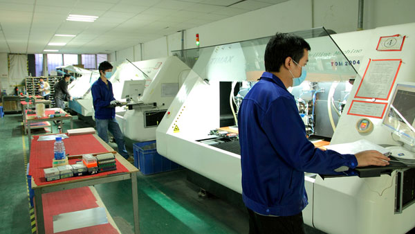
Drilling Machine

CNC Routing Machine

Pressing

X-ray Machine

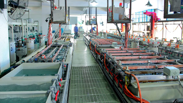
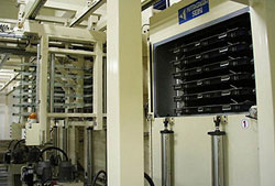
Plating Line

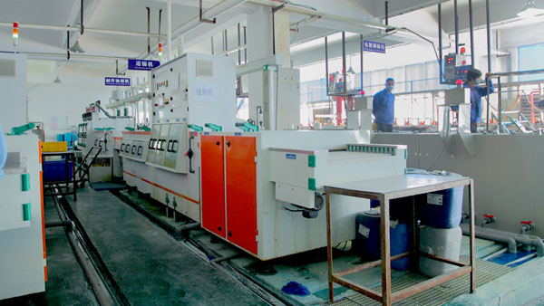
Etching Line

AOI Scanning

AOI Inspection

Silkscreen

Dust-free Room

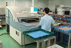
Auto Film Exposure

Auto Gold Immersion Line

Waste Handling 1

Waste Handling 2
")
E-test(E-fixture Test)

Flying Probe Test
")
Flying Probe Test(High Speed)
Bare-board Test2014-08-25
Unpopulated boards may be subjected to a bare-board test where each circuit connection (as defined in a netlist) is verified as correct on the finished board. There are mainly two kinds of electrical t...
Printed Circuit Board Assembly2014-08-25
After the printed circuit board (PCB) is completed, electronic components must be attached to form a functional printed circuit assembly, or PCA (sometimes called a printed circuit board assembly PCBA)...
Protection and Packaging of PCB Assembly2014-08-25
PCBs intended for extreme environments often have a conformal coating, which is applied by dipping or spraying after the components have been soldered. The coat prevents corrosion and leakage currents ...
Circuit Properties of the PCB2014-08-25
Each trace consists of a flat, narrow part of the copper foil that remains after etching. The resistance, determined by width and thickness, of the traces must be sufficiently low for the current the c...
Materials of Printed Circuit Board2014-08-25
Excluding exotic products using special materials or processes all printed circuit boards manufactured today can be built using the following four materials: 1. Laminates 2. Copper-clad laminates 3. Re...
Multiwire Boards2014-08-25
Multiwire is a patented technique of interconnection which uses machine-routed insulated wires embedded in a non-conducting matrix (often plastic resin). It was used during the 1980s and 1990s. Multiwi...
History of Printed Circuit Boards2014-08-25
Development of the methods used in modern printed circuit boards started early in the 20th century. In 1903, a German inventor, Albert Hanson, described flat foil conductors laminated to an insulating ...