In subtractive methods the unwanted copper is removed to leave only the desired copper pattern. In additive methods the pattern is electroplated onto a bare substrate using a complex process. The advantage of the additive method is that less material is needed and less waste is produced.
The pattern in the manufacturer's PCB CAM system is usually output on a photomask (photo-tool, film) by aphotoplotter and replicated via silk screen printing or by exposing on a photo-sensitive photoresist coating. Direct laser imaging techniques are sometimes used for high-resolution requirements.
Subtractive Process
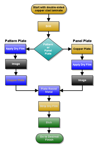
The two processing methods used to produce a double-sided PWB with plated through holes.
Subtractive methods remove copper from an entirely copper-coated board:
Silk screen printing uses etch-resistant inks to protect the copper foil. Subsequent etching removes the unwanted copper. Alternatively, the ink may be conductive, printed on a blank (non-conductive) board.
The latter technique is also used in the manufacture of hybrid circuits.
Photoengraving uses a photomask and developer to selectively remove a photoresist coating. The remaining photoresist protects the copper foil. Subsequent etching removes the unwanted copper.
PCB milling uses a two or three-axis mechanical milling system to mill away the copper foil from the substrate. A PCB milling machine (referred to as a 'PCB Prototyper') operates in a similar way to a plotter, receiving commands from the host software that control the position of the milling head in the x, y, and (if relevant) z axis. Data to drive the Prototyper is extracted from files generated in PCB design software and stored in HPGL or Gerber file format.
Additive Process
Additive processes adds desired copper traces to an insulating substrate. In the full additive process the bare laminate is covered with a photosensitive film which is imaged (exposed to light though a mask and then developed which removes the unexposed film). The exposed areas are sensitized in a chemical bath, usually containing palladium and similar to that used for through hole plating which makes the exposed area capable of bonding metal ions. The laminate is then plated with copper in the sensitized areas. When the mask is stripped, you have a finished PCB.
Semi-additive Process
This is the most common process: The unpatterned board has a thin layer of copper already on it. A reverse mask is then applied. (Unlike a subtractive process mask, this mask exposes those parts of the substrate that will eventually become the traces.) Additional copper is then plated onto the board in the unmasked areas; copper may be plated to any desired weight. Tin-lead or other surface platings are then applied. The mask is stripped away and a brief etching step removes the now-exposed bare original copper laminate from the board, isolating the individual traces. Some single-sided boards which have plated-through holes are made in this way. General Electric made consumer radio sets in the late 1960s using additive boards.
The additive process is commonly used for multi-layer boards as it facilitates the plating-through of the holes to produce conductive vias in the circuit board.
Patterning Method by Volume
The method chosen depends on the number of boards to be produced.
Large Volume
Silk screen printing–the main commercial method.
Photographic methods–used when fine linewidths are required.
Small Volume
Print onto transparent film and use as photomask along with photo-sensitized boards. (i.e., pre-sensitized boards), then etch. (Alternatively, use a film photoplotter).
Laser resist ablation: Spray black paint onto copper clad laminate, place into CNC laser plotter. The laser raster-scans the PCB and ablates (vaporizes) the paint where no resist is wanted. Etch. (Note: laser copper ablation is rarely used and is considered experimental.[clarification needed])
Use a CNC-mill with a spade-shaped (i.e., a flat-ended cone) cutter or miniature end-mill to rout away the undesired copper, leaving only the traces.
Hobbyist
Laser-printed resist: Laser-print onto transparency film, heat-transfer with an iron or modified laminator onto bare laminate, touch up with a marker, then etch.
Vinyl film and resist, non-washable marker, some other methods. Labor-intensive, only suitable for single boards