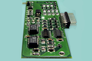
Component manufacturers are continually developing new and smaller packages for components that are mere fractions of a millimeter and have board to component clearances of less than a mil. Pick and place machines have new accessories that allow placement of these almost invisible parts. Components are placed extremely close together. How do you effectively clean under something so small?
No-lead solder is a relatively recent legislated fact of life that necessitated new solder, new fluxes, higher temperatures, and new solder processing equipment. Many new approaches, alloys, chemicals, and soldering processes have been developed to address these issues. Tin whisker problems also increased dramatically. Time-delayed effects, however, often will not show up until a product is out the door and has been in service for even a year or two. The pace of product development covers up some of these time-delayed issues when products are routinely discarded for newer models. For products such as mobile phones, problems don’t often show up because comparatively few people are using a mobile phone that is more than 2-3 years old. Few will spend money for repair when an upgraded feature-rich model is available at a subsidized price. For medical devices, however, the potential for failure is very real, and the effects of failure can be devastating.
Design decisions impact other process steps
The single place where it all comes together and where the supporting elements have to operate properly is the manufacturing floor, but often component manufacturers, board designers, and the device manufacturer are operating independently of one another and this communication void exacerbates the problem. Research shows that many failures are a result of printed circuit boards (PCBs) that are not cleaned enough of contaminants from the manufacturing process. There are design issues that are enabled by the advanced CAD design systems utilized for PCB design.
Sometimes a designer will utilize features such as ultra-close copper pour or fill that puts a ground a few mils from a power bus all over the board. The opportunity for shorts with catastrophic consequences just increased several fold. Many designers have little exposure to the production issues of PCB fabrication or board assembly. It’s important for a board designer to really understand how flux from the hand soldering process of a connector can flow to the microvia that was placed right next to a connector pad. Many decisions one makes in implementing a design will impact the other process steps.
Standards need to be raised for high reliability
IPC, the global trade association serving the printed board and electronics assembly industries, their customers, and suppliers, has a task group devoted to addressing all topics connected with determining the cleanliness levels of unpopulated (bare) printed circuit boards and has established a base standard for cleanliness. The IPC-TM-650 standard sets an acceptable range of 0.1 µg/in2 for military applications (0.65 µg/in2 for general applications) of sodium chloride (NaCl). Is this standard enough to prevent failures, and can present cleaning methods truly clean the boards that are being produced today?
There are a number of myths circulating in the industry:
1. All bare boards coming from the fab house are clean.
2. All components are delivered clean with no contamination issues.
3. Flux will never present any problems and can just be poured onto the board without worrying about heating or the absence of heat, and everything will work out okay.
This is not the reality in manufacturing today. But the assumption of these concepts presents major issues for the manufacturer. A board with hidden residual flux contamination may pass QC and operate properly. After arriving in its operating environment, there may be high humidity and temperature swings that generate condensation, which causes residual flux problems to literally begin to grow and eventually cause leakage paths that will cause failures. The high impedance circuits of today’s micropower electronics are even easier to disrupt with stray voltage sources.