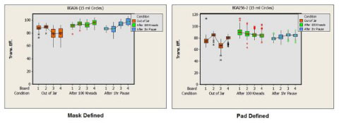
It seems that there is no universal consensus on a seemingly simple choice used in designing electronic circuits. Should the pads on the PCB be defined by the edge of the solder mask opening (mask defined), or should the solder mask opening fall short of the circuit board interconnect (pad or non-solder mask defined)?
Mask-defined BGA traces give more consistent solder paste transfer efficiency. The effect of the gasket formed between the stencil and the solder mask creates a well-defined cavity into which the solder paste deposit is tightly controlled. Figure 1 shows a print volume histogram of two sets of 15 mil (380 micron) diameter circular features on the same board. This means that the printer settings (squeegee speed, pressure, and board/stencil separation speed) were identical. The area ratio of the pad to the stencil aperture wall were the same, and of course, the solder paste was identical.
Figure 1: A print volume histogram of two sets of 15 mil (380 micron) diameter circular features on the same board.
The difference in print volume and print volume repeatability favors the mask defined circles. This test used a 5 mil (125 micron) thick stencil for an area ratio of 0.75. The difference is quite significant to a person who frequently reviews these histograms.